Printed circuit boards form the backbone of modern electronics and effective PCB design is essential for functionality, manufacturability and long-term reliability. While every application has unique needs, several core principles apply across all PCB boards, whether you’re developing single-sided PCB prototypes, complex multi-layer PCBs or flexible assemblies. These five guidelines help maintain performance, reduce production risks and align your work with evolving industry standards.
1. Follow PCB Design Rules and Constraints From the Start
Defining design rules early is crucial for a successful project. These include trace widths, spacing, via sizes, component tolerances and layer stack-up limits. Each parameter should reflect both your manufacturer’s capabilities and your performance goals.
High-speed digital circuits require precise impedance control, while analogue designs need careful signal isolation. Setting these parameters within your CAD software from the outset prevents rework and ensures compliance with IPC standards.
Material properties also play a part. For example, ceramic PCBs demand tighter control over thermal conductivity and expansion coefficients due to their excellent heat resistance and dielectric performance. Ignoring these constraints can cause mechanical stress or delamination during reflow.
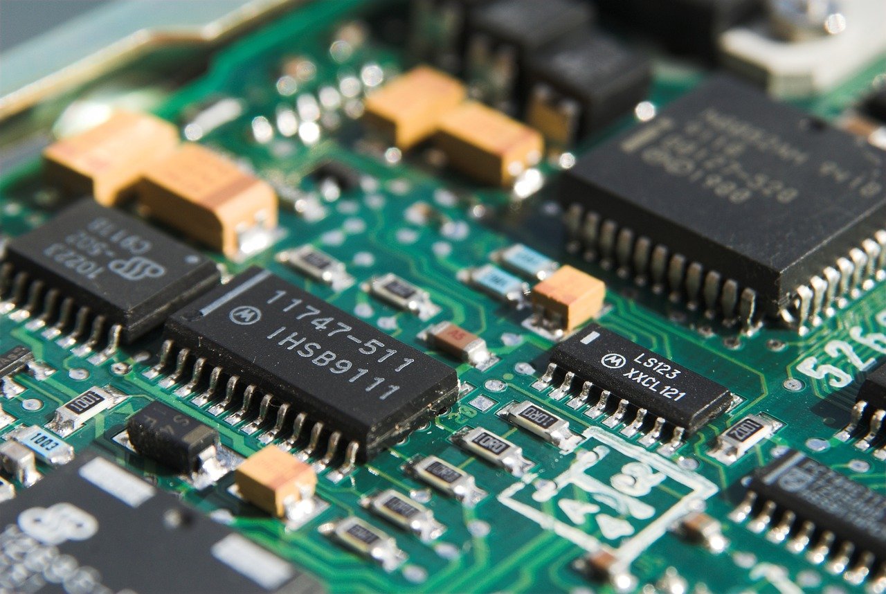
2. Optimise Component Placement With Signal Integrity in Mind
Component placement defines how current flows, how heat spreads and how easy the board is to assemble. Group related parts close together, keep high-speed signals short and align decoupling capacitors with their power pins.
Avoid routing analogue traces near noisy digital lines and maintain clear ground separation where needed. In designs that require enhanced thermal management, metal-core PCBs are often used to help dissipate heat from power components. However, they also limit where parts can be placed, so thoughtful planning at this stage is vital.
A clean, well-structured layout supports both electrical performance and manufacturability, reducing the risk of noise coupling or thermal imbalance later in production.
3. Route Traces Efficiently and Layer Wisely
Once placement is finalised, routing defines the quality and stability of your PCB boards. Keep trace paths short, use 45-degree bends instead of right angles and match lengths on differential pairs for balanced signal timing.
Designers working on double-sided layouts often rely on through-hole vias to interconnect layers, while more complex designs use internal planes to manage power and ground distribution. For flex PCBs, routing must account for bend zones while avoiding vias and sharp turns in areas subject to movement to prevent cracking.
In high-density assemblies, HDI PCBs provide finer routing capability through microvias and thin dielectrics. These designs demand precision but allow for compact, high-performance products with reduced electromagnetic interference. Running quick signal integrity or impedance checks before finalising the layout can confirm routing accuracy and help detect issues early, reducing costly rework during prototyping.
4. PCB Design for Manufacturability and Assembly (DFM & DFA)
A well-designed circuit is only valuable if it can be manufactured efficiently. DFM and DFA principles ensure your PCB design supports both cost control and reliability. Maintain sufficient spacing between pads, avoid excessively small vias and use consistent footprints to simplify automated assembly.
Ensure component orientation is logical and provide test points where practical. For flexible applications, printed flex PCBs introduce additional challenges, such as bend radius control, connector reinforcement and strain relief. Considering these factors early prevents solder fatigue and cracking during use.
Always communicate with your fabrication partner to confirm their tolerances for copper thickness, hole sizes and solder mask clearances. Aligning your design to their process capabilities avoids costly redesigns and delays.
5. Understand the Impact of Emerging Technologies
The pace of innovation in PCB boards continues to accelerate as AI, 5G and automotive systems push for smaller, faster and more efficient designs. New materials and fabrication methods support finer features and tighter tolerances.
Rigid-flex PCBs are increasingly used in aerospace and medical electronics for their ability to integrate rigid sections with flexible connectors, reducing weight and improving reliability. Meanwhile, UHDI and substrate-like PCBs are redefining miniaturisation through ultra-fine geometries that blur the line between PCBs and semiconductor packaging.
As technology advances, mastering DFM principles, stack-up design and high-density routing is essential for maintaining signal integrity and manufacturability.
From Simple to Complex: A Historical Perspective
Understanding how PCB design has evolved helps explain the increasing sophistication of modern electronics. Early PCB boards were simple, supporting few components and limited routing. As functionality demands grew, engineers added conductive layers on both sides of the substrate, improving signal flow and circuit density.
The move to multi-layer architectures transformed performance, creating separate planes for power and ground and enabling compact, high-efficiency assemblies. Advances in materials and manufacturing, including high-temperature laminates and embedded components, have since expanded what’s possible. Each evolution in PCB design reflects the balance between performance, durability and production efficiency.
Modern Design Challenges in PCB Design
Modern PCB boards must meet increasingly demanding electrical, mechanical and environmental standards. Designers face constant pressure to reduce size while maintaining performance, particularly in aerospace, automotive and communication systems. Achieving this balance requires careful attention to materials, heat management and assembly processes from the earliest stages of development.
A strong grasp of PCB design principles ensures that engineers can account for electromagnetic interference, controlled impedance and manufacturability without compromising function. The best results come from understanding how every design choice, from stack-up configuration to trace geometry, affects reliability and cost.
Professional development is critical in this context. Training in soldering, inspection and design for manufacture enables teams to apply technical knowledge effectively when working with complex or high-density double-sided PCBs and other advanced PCB boards.
Strengthen Your Skills With Professional Training
Even as design software grows more powerful, the effectiveness of any PCB design ultimately depends on human expertise. Engineers who combine theoretical knowledge with practical understanding of assembly, inspection and fault analysis are best placed to ensure consistent results.
A.R.T. delivers IPC‑accredited Certified Interconnect Designer (CID) and advanced CID+ (“CID plus”) training programmes focused specifically on PCB design. Covering stack‑up planning, controlled impedance, high‑speed layout, DFM/DFA, and documentation to IPC standards, these courses help design teams produce reliable, manufacturable boards.
As components shrink and systems become more interconnected, maintaining expertise in PCB design methods is essential. Continuous training helps engineers and technicians adapt to new materials, technologies and industry standards, ensuring that every project achieves dependable, production-ready outcomes.
Contact Advanced Rework Technology Today
What could be a better way to start your career as PCB designer rather than getting expertise in globally known IPC standards? If you currently do not have globally recognized IPC certification in your institute or on your resume and you want to make that superior change, contact Advanced Rework Technology (A.R.T.) today. A.R.T Ltd also offers bespoke training that can be based entirely around the requirement of your company and even specific products, with all theory and practical equipment supplied by them too. All is just a call away from you. Call A.R.T. Ltd today on 01245 237 083.
Interested in More Information?
Call: +44 (0)1245 237083
Email: [email protected]
