For organisations operating in aerospace, defence, automotive and other high-reliability sectors, structured PCB design courses play a critical role in preventing avoidable manufacturing failures. Decisions made during layout directly influence solderability, inspection outcomes and long-term field performance. When those choices are made without a clear understanding of fabrication and assembly constraints, the cost of correction can escalate quickly.
High-quality training helps engineers connect design intent with real manufacturing conditions. Rather than focusing solely on layout software tools, effective instruction examines how copper distribution, pad geometry and routing strategy affect downstream processes. Strengthening this understanding at an early stage, particularly through in-depth PCB design training, helps minimise rework, improve first-pass yield and build confidence before committing to production.
Why PCB Design Matters in High-Reliability Manufacturing
Modern electronic assemblies are increasingly compact and complex. As layer counts increase and component sizes shrink, tolerance for layout error decreases. In this context, disciplined layout practice supports predictable fabrication and consistent inspection performance.
Early learning in structured PCB design often begins with comparison of simple constructions, such as a single-sided board, before progressing to multi-layer architectures. Understanding how complexity evolves gives engineers a perspective on why careful planning prevents downstream issues.
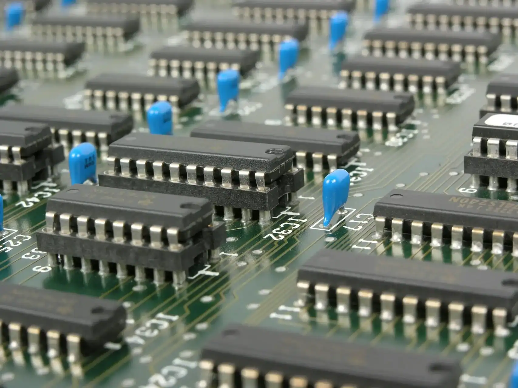
Connectivity strategy is equally important. The role of a plated through hole in linking conductive layers highlights how small structural features influence electrical continuity and mechanical integrity. These are not purely fabrication concerns; they originate from informed decisions made during layout.
Core Principles in Professional PCB Design
Effective PCB design courses emphasise practical fundamentals rather than abstract theory. Stack-up planning, material selection and routing discipline form the backbone of reliable layout development. Engineers learn how conductor width, spacing and return paths affect signal integrity and electromagnetic compatibility. This structured approach ensures that design decisions remain aligned with both electrical performance and manufacturability requirements.
Management of track spacing is particularly important in dense layouts. Insufficient clearance can introduce cross-talk or compromise inspection criteria. Strong design practice therefore, incorporates rule setting and verification that reflect real fabrication capability. By validating constraints early, teams reduce the likelihood of late-stage redesign or production delays.
Thermal behaviour is another critical factor. Designers must understand how copper distribution influences solder joint formation and stress. Inadequate planning during PCB design can result in inconsistent wetting or component damage during assembly. Careful evaluation of heat flow across planes and pads improves both reliability and repeatability in manufacture.
Documentation also plays a central role. Accurate engineering drawing preparation ensures that component placement and orientation are interpreted correctly on the production floor. Clear documentation supports traceability and reduces inspection delays. It also provides a reference point for quality teams when verifying that assemblies meet defined acceptance criteria.
PCB Design and IPC Standards Alignment
For companies and organisations working to IPC standards, alignment between layout practice and inspection expectations is essential. Professional instruction reinforces how design decisions influence compliance with IPC-A-600 and IPC-A-610 acceptance criteria.
Designers who understand inspection requirements can incorporate those expectations directly into their process, ensuring assemblies are prepared for final inspection without unnecessary rework. Integrating these criteria early into PCB design reduces ambiguity in acceptance standards and supports more consistent build quality. This proactive alignment strengthens quality control before boards enter volume manufacture and helps prevent avoidable non-conformances.
At A.R.T., structured training is delivered by Master IPC Trainers who actively participate in IPC task groups. Their involvement ensures that learning reflects current standards development and practical industry requirements. Participants in IPC training courses gain insight into how layout parameters connect to inspection outcomes and long-term reliability.
Practical Manufacturing Considerations in PCB Design
The practical value of structured training becomes clear when layouts are translated into physical assemblies. Decisions made during PCB design determine how easily boards can be assembled, tested, and, if necessary, modified.
Thermal management provides a practical example. Awareness of copper balancing during layout supports appropriate process planning during assembly, including controlled preheating before soldering. Understanding heat distribution reduces stress and improves joint consistency, particularly in high-density or multi-layer constructions.
Repair considerations are also shaped by early design choices. Layouts that restrict access or fail to account for thermal balance can complicate modification work and extend downtime. Insights drawn from programmes, such as the Rework C1 course, demonstrate how thoughtful PCB design reduces the likelihood of difficult or intrusive repairs.
Effective planning therefore, anticipates the entire lifecycle of a board, from fabrication through to maintenance, strengthening long-term reliability and serviceability.
Who Benefits From PCB Design?
Structured training programmes are valuable for graduate engineers building core layout competence, experienced designers moving into regulated industries and quality managers who need clearer visibility of design-related risk. Manufacturing engineers also benefit from a stronger understanding of how layout decisions influence fabrication and inspection, as this improves communication between design, quality and production teams.
In aerospace and defence applications, disciplined PCB design is closely linked to compliance with demanding environmental and acceptance standards. Consistency in documentation, routing strategy and manufacturability assessment reduces variation between projects and strengthens overall process control.
As the longest-running IPC Certification Centre in the UK, with members active on IPC task groups, A.R.T. delivers courses grounded in practical industry experience. This ensures that training reflects real manufacturing pressures, including the realities of final inspection, supporting reliable outcomes across complex electronics programmes.
Strengthening Reliability Through Structured PCB Design Education
Ultimately, the objective of PCB design courses is to embed reliability at the earliest stage of product development. When engineers understand how layout decisions affect solderability, inspection and durability, they reduce the likelihood of costly redesign cycles.
A structured approach to PCB design protects margins, shortens development timelines and improves confidence before production release. By investing in structured courses, companies build a stable foundation for predictable manufacturing performance. This early commitment to robust layout practice reduces late-stage redesign and strengthens collaboration between design, quality and production teams.
To explore how Advanced Rework Technology supports capability in PCB design, review the full range of accredited programmes available. Through practical instruction and standards alignment, A.R.T. continues to deliver PCB design courses that strengthen reliability where it matters most.
Interested in More Information?
Call: +44 (0)1245 237083
Email: [email protected]
