Through-hole technology is a method of mounting electronic components by inserting their leads into holes drilled in a printed circuit board (PCB). These leads are then soldered to pads on the opposite side of the board, creating a strong electrical and mechanical connection. While surface mount technology (SMT) is more common in high-volume manufacturing settings, through-hole technology remains a reliable option for assemblies that demand physical strength, thermal resilience or field serviceability.
Before exploring how it works, it is worth noting that technicians and engineers benefit significantly from hands-on instruction when learning or applying soldering methods. A.R.T. offers a range of electronics training courses that include component mounting, joint quality inspection and soldering skills for both SMT and through-hole work.

Interested in More Information on PCBs?
Call: +44 (0)1245 237083
Email: [email protected]
Understanding Through-Hole Technology in PCB Assembly
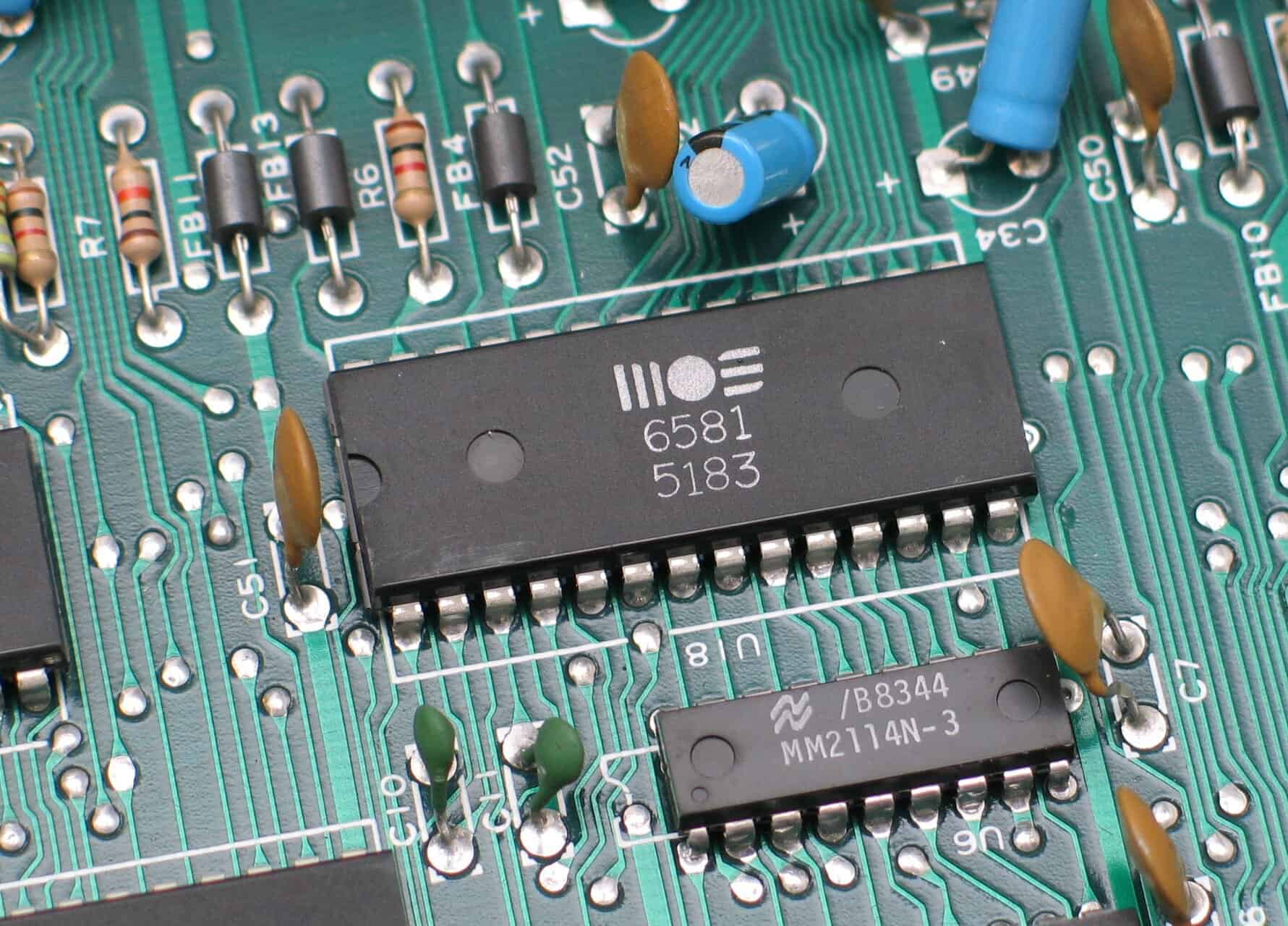
At their core, through-hole technologies involve placing component leads through drilled holes in the PCB and soldering them to pads on the opposite side. Unlike surface-mounted components, which sit directly on top of the board, through-hole components offer a more secure bond and are physically anchored into place.
This method is particularly valuable in environments where PCBs are subjected to shock, vibration or mechanical stress. For this reason, through-hole technology is still widely used in aerospace, defence, transportation and industrial controls. It is also preferred in test and development environments where components may need to be replaced manually.
How Through-Hole Components Are Used
There are two main types of through-hole components: those with axial leads and those with radial leads. Axial components, such as resistors, have leads that extend from both ends, while radial components, such as certain capacitors, have both leads extending from one side.
Through-hole technology is commonly used for connectors, transformers, high-power resistors and other parts that require greater mechanical support or higher current handling. It is also helpful during prototyping, where components may need to be easily changed or adjusted. In some assemblies, both sides of the board are soldered to secure tall or heavy components more effectively.

The Soldering Process for Through-Hole Technology
Soldering in through-hole technology can be performed manually or via wave soldering. Manual soldering involves inserting the component leads through the holes, trimming any excess, and applying heat and solder to form a secure joint. In wave soldering, the entire underside of the PCB is passed over a wave of molten solder after components are placed and fixed.
Each joint must meet defined acceptance criteria, including proper fill of the plated hole, visible wetting to both lead and pad, and a smooth solder fillet. The solder must rise to a defined height without exceeding acceptable lead protrusion. Please review common PCB soldering issues. Additionally, these inspection points are outlined in IPC-A-610, which sets clear standards for Class 2 (general electronics) and Class 3 (high-reliability electronics) assemblies.
Maintaining consistent joint quality in through-hole technology requires attention to thermal mass, solder flow and lead alignment. Variations in lead diameter or hole size can also create challenges, especially in mixed-technology boards.
Benefits of Through-Hole Technology
One of the most significant advantages of through-hole technology is its mechanical strength. Because the leads pass through the board and are soldered on the opposite side, the resulting joints are more robust and better able to withstand physical stress. This is particularly important for parts that may be handled, adjusted or connected frequently.
Through-hole components are easier to inspect and replace than many surface-mounted alternatives. They are also less likely to become dislodged during manual assembly or rework. These characteristics make them ideal for mission-critical applications, such as military avionics or industrial power supplies, where component failure is unacceptable.
Their size and visibility also make them a valuable teaching aid for trainees learning soldering and inspection fundamentals. In practical training environments, through-hole components provide a clear view of joint formation, lead trimming and wetting behaviour, helping new technicians build confidence before progressing to more compact or automated technologies.
Limitations of Through-Hole Technology
Despite its strengths, through-hole technology is not without drawbacks. It generally requires more manual labour and time than SMT and adds complexity to PCB design by occupying space on both sides of the board. Drilled holes reduce the available area for routing signal traces and increase manufacturing costs.
For high-density, compact devices such as mobile phones or tablets, through-hole technology is rarely used. Instead, it is applied selectively in assemblies that require specific component properties, often alongside SMT in a mixed-technology layout.
Training and Inspection for Through-Hole Soldering
Given the critical role that through-hole technology plays in many high-reliability systems, proper training is essential. Technicians must be able to identify defects such as insufficient solder fill, cold joints, excessive lead protrusion and improper wetting.
Hands-on instruction helps reinforce correct soldering techniques and conformal coatings for PCBs. Additionally, inspection methods aligned with IPC-A-610. A.R.T.’s IPC A610 training ensures participants understand the visual and measurable requirements for through-hole joints at both Class 2 and Class 3 levels.
In addition to standards knowledge, training helps develop the judgement needed to work with real-world variations in board condition, component tolerances and production constraints. Building this capability is vital for quality assurance teams and technicians involved in assembly, inspection or rework. This hands-on experience supports a deeper understanding of soldering principles that can be applied across different assembly methods.
Conclusion: The Lasting Value of Through-Hole Technology
Although often overshadowed by surface mounting, through-hole technologies continue to deliver value in assemblies that demand strength, reliability and long service life. The role of such technology in supporting mission-critical electronics, high-current connections and user-accessible components remains should, therefore, not be overlooked.
For anyone working with or inspecting assemblies that include this mounting method, understanding the process, standards and challenges of through-hole technology is key to achieving reliable results. For newcomers or those looking to formalise their skills, our course C1 PCB provides the foundation needed to build confidence and capability.
Through focused instruction, structured inspection and ongoing practical experience, manufacturers can continue to benefit from the unique strengths of through-hole technology while maintaining the high standards expected across regulated industries.
